arduino atmega328p datasheet pdf - Typical values contained in this datasheet are based on simulations and characterization of actual ATmega328P AVR microcontrollers manufactured on the typical process technology.
Automotive min and max values are based on characterization of actual ATmega328P AVR microcontrollers manufactured on the whole process excursion (corner run).
The Atmel ATmega328P is a low-power CMOS 8-bit microcontroller based on the AVR enhanced RISC architecture. By executing powerful instructions in a single clock cycle, the ATmega328P achieves throughputs approaching 1MIPS per MHz allowing the system designer to optimize power consumption versus processing speed.
During reset, all I/O registers are set to their initial values, and the program starts execution from the reset vector.
For the Atmel ATmega328P, the instruction placed at the reset vector must be an RJMP – relative jump – instruction to the reset handling routine.
If the program never enables an interrupt source, the interrupt vectors are not used, and regular program code can be placed at these locations.
This is also the case if the reset vector is in the application section while the interrupt vectors are in the boot section. The circuit diagram in Figure 10-1 shows the reset logic.
The I/O ports of the AVR are immediately reset to their initial state when a reset source goes active. This does not require any clock source to be running.
After all reset sources have gone inactive, a delay counter is invoked, stretching the internal reset. This allows the power to reach a stable level before normal operation starts.
The time-out period of the delay counter is defined by the user through the SUT and CKSEL fuses. The different selections for the delay period are presented in Section 8.2 “Clock Sources” on page 25 (see the datasheet).
Reset Sources

The same applies when changing drive value (if configured as output) or enabling/disabling of pull-up resistors (if configured as input). Each output buffer has symmetrical drive characteristics with both high sink and source capability.
The pin driver is strong enough to drive LED displays directly. All port pins have individually selectable pull-up resistors with a supply-voltage invariant resistance.
All I/O pins have protection diodes to both VCC and Ground as indicated in Figure 13-1 (see the datasheet). Refer to Section 28. “Electrical Characteristics” on page 258 for a complete list of parameters.
 All registers and bit references in this section are written in general form. A lower case “x” represents the numbering letter for the port, and a lower case “n” represents the bit number.
However, when using the register or bit defines in a program, the precise form must be used. For example, PORTB3 for bit no. 3 in port B, here documented generally as PORTxn.
The physical I/O registers and bit locations are listed in Section 13.4 “Register Description” on page 72.
Three I/O memory address locations are allocated for each port, one each for the data register – PORTx, data direction register – DDRx, and the port input pins – PINx.
The port input pins I/O location is read only, while the data register and thedata direction register are read/write. However, writing a logic one to a bit in the PINx register, will result in a toggle in the corresponding bit in the data register.
In addition, the pull-up disable – PUD bit in MCUCR disables the pull-up function for all pins in all ports when set.
Using the I/O port as general digital I/O is described in Section 13.2 “Ports as General Digital I/O” on page 59.
Most port pins are multiplexed with alternate functions for the peripheral features on the device.
How each alternate function interferes withthe port pin is described in Section 13.3 “Alternate Port Functions” on page 63.
Refer to the individual module sections for a full description of the alternate functions. Note that enabling the alternate function of some of the port pins does not affect the use of the other pins in the port as general digital I/O.
You can download Arduino ATmega328p datasheet (PDF) here.
Automotive min and max values are based on characterization of actual ATmega328P AVR microcontrollers manufactured on the whole process excursion (corner run).
The Atmel ATmega328P is a low-power CMOS 8-bit microcontroller based on the AVR enhanced RISC architecture. By executing powerful instructions in a single clock cycle, the ATmega328P achieves throughputs approaching 1MIPS per MHz allowing the system designer to optimize power consumption versus processing speed.
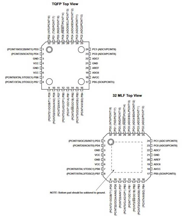
ATmega328p Pin Configurations
System Control and Reset
Resetting the AVRDuring reset, all I/O registers are set to their initial values, and the program starts execution from the reset vector.
For the Atmel ATmega328P, the instruction placed at the reset vector must be an RJMP – relative jump – instruction to the reset handling routine.
If the program never enables an interrupt source, the interrupt vectors are not used, and regular program code can be placed at these locations.
This is also the case if the reset vector is in the application section while the interrupt vectors are in the boot section. The circuit diagram in Figure 10-1 shows the reset logic.
The I/O ports of the AVR are immediately reset to their initial state when a reset source goes active. This does not require any clock source to be running.
After all reset sources have gone inactive, a delay counter is invoked, stretching the internal reset. This allows the power to reach a stable level before normal operation starts.
The time-out period of the delay counter is defined by the user through the SUT and CKSEL fuses. The different selections for the delay period are presented in Section 8.2 “Clock Sources” on page 25 (see the datasheet).
Reset Sources
- The Atmel ATmega328P has four sources of reset:
- Power-on reset. The MCU is reset when the supply voltage is below the power-on reset threshold (VPOT).
- External reset. The MCU is reset when a low level is present on the RESET pin for longer than the minimum pulse length.
- Watchdog system reset. The MCU is reset when the watchdog timer period expires and the watchdog system reset mode is enabled.
- Brown-out reset. The MCU is reset when the supply voltage VCC is below the brown-out reset threshold (VBOT) and the brown-out detector is enabled.
ATmega328p I/O-Ports
All AVR ports have true read-modify-write functionality when used as general digital I/O ports. This means that the direction of one port pin can be changed without unintentionally changing the direction of any other pin with the SBI and CBI instructions.The same applies when changing drive value (if configured as output) or enabling/disabling of pull-up resistors (if configured as input). Each output buffer has symmetrical drive characteristics with both high sink and source capability.
The pin driver is strong enough to drive LED displays directly. All port pins have individually selectable pull-up resistors with a supply-voltage invariant resistance.
All I/O pins have protection diodes to both VCC and Ground as indicated in Figure 13-1 (see the datasheet). Refer to Section 28. “Electrical Characteristics” on page 258 for a complete list of parameters.
ATmega328p I/O Pin Equivalent Schematic
However, when using the register or bit defines in a program, the precise form must be used. For example, PORTB3 for bit no. 3 in port B, here documented generally as PORTxn.
The physical I/O registers and bit locations are listed in Section 13.4 “Register Description” on page 72.
Three I/O memory address locations are allocated for each port, one each for the data register – PORTx, data direction register – DDRx, and the port input pins – PINx.
The port input pins I/O location is read only, while the data register and thedata direction register are read/write. However, writing a logic one to a bit in the PINx register, will result in a toggle in the corresponding bit in the data register.
In addition, the pull-up disable – PUD bit in MCUCR disables the pull-up function for all pins in all ports when set.
Using the I/O port as general digital I/O is described in Section 13.2 “Ports as General Digital I/O” on page 59.
Most port pins are multiplexed with alternate functions for the peripheral features on the device.
How each alternate function interferes withthe port pin is described in Section 13.3 “Alternate Port Functions” on page 63.
Refer to the individual module sections for a full description of the alternate functions. Note that enabling the alternate function of some of the port pins does not affect the use of the other pins in the port as general digital I/O.
Atmega 328P Pin Explanation
You can download Arduino ATmega328p datasheet (PDF) here.
Comments
Post a Comment